| REGISTER-LOGIN | PRODUCTS | CROSS REFERENCE | INVENTORY | REQUEST QUOTE | ORDER ONLINE | SITE MAP |
| SMS112 - FLIP CHIP | |
| GOLD CHIP TECHNOLOGY™ | 150mA LOW DROPOUT VOLTAGE REGULATOR WITH ON/OFF SWITCH |
| FEATURES | APPLICATIONS | 150mA Low Drop Voltage Regulators - FLIP CHIP |
|
3.3V and 5V Voltage Available Active High On/Off Control Output Current of 150mA Very Low Quiescent Current Low Dropout Voltage of 80mV at 30mA Very Low Noise Short Circuit Protection Internal Thermal Shutdown Space Saving 5 Lead SOT-23 Package High reliability Unique new design in 0603 style case Gold metallization RoHS compliant, Lead Free Compatible with both chip and wire, flip chip and surface mount assembly. |
Battery Powered Systems Portable Consumer Equipment Cordless Telephones Portable (Notebook) Computers Portable Instrumentation Radio Control Systems Personal Communication Equipment Toys Low Voltage Systems Chip on Board System in package SIP Hybrid Circuits |
|
| 150mA LOW DROPOUT VOLTAGE REGULATOR WITH ON/OFF SWITCH - PRODUCT DESCRIPTION |
|
The AMS112 series consists of positive fixed voltage regulators featuring an internal electronic switch controlled by TTL or CMOS logic levels. When the Control pin is pulled to a logic high level, the device is in the ON state. If the control function is not used, the control terminal should be connected to a logic high level or VIN, therefore allowing the regulator to be ON. The regulator will be ON when the control terminal voltage is grater than 1.8V. To lower the output noise level to 30mVrms, an external capacitor can be connected to the noise bypass pin. These devices feature very low quiescent current of 1mA when supplying 30mA loads (180mA at no load). This unique characteristic and the low standby current (typ. 100nA) make the AMS112 ideal to use for standby power systems. Like other regulators the AMS112 series also includes internal current limiting and thermal shutdown. The AMS112 is offered in 3.3V and 5.0V output voltages, and is available in the 5-pin SOT-23 surface mount package. Flip Chip Low Drop Voltage Regulators Integrated Circuits series are available in die form in four different pad compositions: -FC, -GB, -GT and -AN. These products are ideal for high reliability hybrid circuits, multi chip module applications and surface mount applications. |
| HIGH RELIABILITY BARE DIE AND SYSTEM IN PACKAGE - SHORT APPLICATION NOTE |
| COB (Chip on Board) and SiP (System-in-Package) are integrating proven mature products in bare die of mixed technologies i.e. Si, GaAs, GaN, InP, passive components, etc that cannot be easily implemented in SOC (System-on-Chip) technology. COB and SiP have small size footprint, high density, shorter design cycle time, easier to redesign and rework, use simpler and less expensive assembly process. For extreme applications the bare die has to withstand also harsh environmental conditions without the protection of a package. KGD, Known Good Die concept is no longer satisfactory if the die cannot withstand harsh environmental conditions and degrades. Standard semiconductor devices supplied by many manufacturers in bare die are build with exposed aluminum pads that are extremely sensitive to moisture and corrosive components of the atmosphere. Semiconix has reengineered industry standard products and now offers known good die for bare die applications with gold interconnection and well-engineered materials that further enhance the die reliability. Semiconix also offers Silicon Printed Circuit Board technology with integrated passive components as a complete high reliability SIP solution for medical, military and space applications. See AN-SMX-001 |
| DISCRETE SEMICONDUCTORS MANUFACTURING PROCESS |
| Discrete semiconductors are manufactured using Semiconix in house high reliability semiconductor manufacturing processes. All semiconductor devices employ precision doping via ion implantation, silicon nitride junction passivation, platinum silicided contacts and gold interconnect metallization for best performance and reliability. MNOS capacitors, Tantalum Nitride TaN or Sichrome SiCr thin film resistors are easily integrated with discrete semiconductors on same chip to obtain standard and custom complex discrete device solutions. |
| ABSOLUTE MAXIMUM RATINGS @ 25 °C (unless otherwise stated) | |||
| Parameter | Symbol | Value | Unit |
| Power Dissipation | 400 | mW | |
| Input Voltage | 16 | V | |
| Storage Temperature | -55 to +150 | °C | |
| Operating Junction Temperature | -30°C to +80 | °C | |
| Electrical Characteristics* at IOUT=0 mA, TC=25°C unless otherwise noted | ||||||
| Name | Symbol | Test Conditions | Value | Unit | ||
| Min. | Typ. | Max | ||||
| Output Voltage (Note 2) | VIN=VOUT+1V | -3 | 3 | % | ||
| Standby Current | VIN=8V, at output off | 0.1 | mA | |||
| Line Regulation | V IN=VOUT+1V to VOUT+6V | 3 | 20 | mV | ||
| Load Regulation, (Notes 2, 3) | 5mA≤IO≤60mA | 10 | 50 | mV | ||
| Dropout Voltage (VIN - VOUT) | IO=60 mA | 160 | 260 | mV | ||
| Dropout Voltage (VIN - VOUT) | IO=150 mA | 290 | 400 | mV | ||
| Quiescent Current | IO=0 mA, Except ICONT | 170 | 350 | mA | ||
| Ripple Rejection | 100mVrms, IO=10mA | 55 | dB | |||
| Output Noise Voltage | 10Hz < f < 80kHz, IO=30mA | 30 | mVrms | |||
| Temperature Coefficient | IO=10mA, -20°C≤TA≤+75°C | 0.2 | mV/°C | |||
| Noise Bypass Terminal Voltage | 1.25 | V | ||||
| On/Off Current | Output On | 12 | 30 | mA | ||
| On/Off Voltage | Output On | 1.8 | V | |||
| On/Off Voltage | Output Off | 0.6 | V | |||
| Output Rise Time | IO=30 mA, VCONT=0V to 1.8V | 0.3 | ms | |||
| SPICE MODEL | ||||||
| Spice model pending. | ||||||
| CROSS REFERENCE PARTS: AMS Advanced Monolithic Systems AMS112 | ||||||
| GENERAL DIE INFORMATION | ||||||||||||||||||||||||
| Substrate | Thickness [mils] |
Size LxW[mils] |
Bonding pads dimensions per drawing | Backside | ||||||||||||||||||||
| Silicon Si |
10±2 |
30x30±1 [0.76x0.76±0.025] |
|
Optional backside coating and/or marking. | ||||||||||||||||||||
| LAYOUT / DIMENSIONS / PAD LOCATIONS | ||||||
|
||||||

|
|
|||||
 |
||||||


| APPLICATION HINTS |
APPLICATION HINTS |
|
| Figure 1: Pinout |
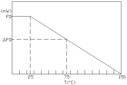 |
| Figure 2: Power Dissipation |
| SEMICONDUCTOR ASSEMBLY PROCESS - SHORT APPLICATION NOTE |
|
Semiconix flip chip components are designed for dry assembly processes as well as for processes that use adhesives, fluxes etc. Dry assembly
process is an assembly process that does not use additional solders, fluxes or adhesives. Thermosonic wire bonding is a dry assembly process.
Semiconix Flip Chip -FC series can be also used for thermosonic wire bonding. Semiconix Gold Bump -GB series are flip chips that are thermosonically
attached to a circuit. Semiconix Gold Tin -GT series are flip chips with Au/Sn, 80/20 metallized pads. GT series can be attached to circuits by
bringing the die in contact with a substrate which temperature is more than 280°C. Upon cooling bellow 280C, the die is firmly welded to the
substrate. Flux less dry assembly is most reliable but is also most expensive because of thick gold bumps or expensive Au/Sn process. Semiconix -FC series is designed to be used for flip chip assembly with conductive silver epoxy. It is a simple and inexpensive process consisting of 3 steps: - transfer a thin conductive epoxy layer onto the bonding pads; -align to substrate and attach; -cure silver epoxy and inspect. Same procedure may be used also with -GB series in certain applications. Semiconix Gold/Nickel -AN series is the most efficient wafer level chip size package W-CSP designed for mixed surface mount and flip chip applications. The assembly process is same as for packaged surface mount components. The process consist of at least 3 steps; -screen print solder paste on the printed circuit board; -flip chip, align and attach to the tacky solder paste; -dry paste, reflow at T>220°C, clean, etc. Semiconix Flip Chip -AN series are available in many sizes with landing pads compatible with the industry standard CSP as well as surface mount packages. |
| STANDARD PRODUCTS ORDERING INFORMATION |
| VERSION | SMX P/N | WAFFLE PACKS | QUANTITY | U/P($) | FILM FRAME | MIN QUANTITY | U/P($) |
| Flip chip | SMS112-FC | -WP | 1000 | -FF | 1000 | ||
| Flip chip | SMS112-FC | -WP | 5000 | -FF | 5000 | ||
| Gold Bump | SMS112-GB | -WP | 1000 | -FF | 1000 | ||
| Gold Bump | SMS112-GB | -WP | 5000 | -FF | 5000 | ||
| Gold-Tin | SMS112-GT | -WP | 1000 | -FF | 1000 | ||
| Gold-Tin | SMS112-GT | -WP | 5000 | -FF | 5000 | ||
| Gold/Nickel | SMS112-AN | -WP | 1000 | -FF | 1000 | ||
| Gold/Nickel | SMS112-AN | -WP | 5000 | -FF | 5000 |
| PRICES - Listed prices are only for standard products, available from stock. Inventory is periodically updated. List prices for other quantities and tolerances are available on line through Instant Quote. For standard products available from stock, there is a minimum line item order of $550.00. No rights can be derived from pricing information provided on this website. Such information is indicative only, for budgetary use only and subject to change by SEMICONIX SEMICONDUCTOR at any time and without notice. |
| LEAD TIMES - Typical delivery for standard products is 4-6 weeks ARO. For custom devices consult factory for an update on minim orders and lead times. |
| CONTINOUS SUPPLY - Semiconix guarantees continuous supply and availability of any of its standard products provided minimum order quantities are met. |
| CUSTOM PRODUCTS - For custom products sold as tested, bare die or known good die KGD, there will be a minimum order quantity MOQ. Dice are 100% functional tested, visual inspected and shipped in antistatic waffle packs. For high volume and pick and place applications, dice are also shipped on film frame -FF. For special die level KGD requirements, different packaging or custom configurations, contact sales via CONTACTS page. |
| SAMPLES - Samples are available only for customers that have issued firm orders pending qualification of product in a particular application. |
| ORDERING - Semiconix accepts only orders placed on line by registered customers. On line orders are verified, accepted and acknowledged by Semiconix sales department in writing. Accepted orders are non cancelable binding contracts. |
| SHIPING - Dice are 100% functional tested, visual inspected and shipped in antistatic waffle packs. For high volume and pick and place applications, dice are also shipped on film frame -FF. |
| DISCLAIMER - SEMICONIX has made every effort to have this information as accurate as possible. However, no responsibility is assumed by SEMICONIX for its use, nor for any infringements of rights of third parties, which may result from its use. SEMICONIX reserves the right to revise the content or modify its product line without prior notice. SEMICONIX products are not authorized for and should not be used within support systems, which are intended for surgical implants into the body, to support or sustain life, in aircraft, space equipment, submarine, or nuclear facility applications without the specific written consent. |
| HOME | PRODUCT TREE | PACKAGES | PDF VERSION | SEARCH |
| SEMICONIX SEMICONDUCTOR | www.semiconix-semiconductor.com Tel:(408)758-8694 Fax:(408)986-8027 |
SEMICONIX SEMICONDUCTOR |
| Last updated:July 06, 2009 | Display settings for best viewing: | Current display settings: |
| Page hits: 1 | Screen resolution: 1124x864 | Screen resolution: |
| Total site visits: | Color quality: 16 bit | Color quality: bit |
| © 1990-2024 SEMICONIX SEMICONDUCTOR All rights reserved. No material from this site may be used or reproduced without permission. | ||